|
|
|
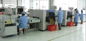
PCB Production Line...
Defence electronics demands very high performance and operational environment parameters on all production products (in
the main). To that end we use sophisticated CAD software to design and simulate all of our electronics circuits and software
programs - including that of microcode and FPGAs etc. We then optimise and design the PCBs we need, and can
handle up to 16 layer boards currently and half a metre square! That said we can design a small ceramic substrate PCB of less
than 2mm square.... Given the special coatings and silver plating we currently enjoy good supplier relationships
and have nearly all of the PCBs etched and coated externally to the Company. We continue to explore bringing more of the specialist
materials end of this in-house and for now this makes little economic sense. We can't see us ever bringing this completely
'in-house'. All boards are coded and are 100% fully tested (not batch tested), and we barcode each so they are unique
and can be carefully managed in the production and thence supply chain. We are currently working with UK's Leading Production Specialist and highly respected supplier to specify for us a 100% fully automated PCB production line from initial scanning,
solder paste 'printing', high speed component placement, vacuum vapour phase oven, conformal coating
and UV cure, and associated workstations for inspection and other component placement and handling. The heart of this is the
component placement system which can handle up to 23,000 surface mount components an hour or a little over six a second! Perhaps
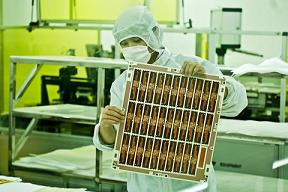
a better way of describing this is that this production line will have the capacity to do around a million full sized boards a
year... and a full-sized board is often made up of multiple copies of the same actual sized PCB from the product or its entire collection
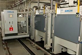
of PCBs. Next comes cleaning of the PCBs for aviation, space or military grade needs - and for that you need
one of the world's most complex cleaning systems to ensure particulate, flux residue and other debris are removed
to ensure the highest possible reliability is achieved for the PCBs and devices. Conformal coatings can be added to ensure
zero oxidation or high humidity or non-ideal environments can be handled such as outdoors or in submarines. Then
you might want to barcode key devices and PCBs uniquely and for that we have designed in specialist laser equipment to write
to 7.5mil (0.19mm) barcodes such as a 32 word x each word of 8 bits data matrix (some 1.5mm x 6mm barcode!) and complementary
readers so that the supply chain can manage traceability to the component level. Then this laser doesn't need to always
write barcodes but can write absolutely tiny features into a composite device or filter. Given the above will
be an expensive investment in the short-term the huge benefit of this is the excess capacity will be sold on to other aerospace,
defence, telecommunication and education establishments. The state-of-the-art production line will be supported with fully-automated
component robotic storage units so that production costs can be kept to an absolute minimum. Reel handling is a sizable
part of an automatic assembly line - and in a fully traceable line (to the component level) this can easily become highly
labour-intensive - hence the robotic storage is a key part to ensure such an assembly line can be competitive based in
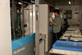
the UK. With inspection being a key part in the verification process we are currently looking at improving
our current approaches with the introduction of state-of-the-art X-ray equipment that can detect non-compliance or early
failure modes in complex PCB soldering fabrication like large BGAs and other similar high-density lead components. This is
also why we are adopting the expensive vacuum vapour phase ovens rather than the non-vacuum - as the vacuum-based ovens
offer much better MTBF and MTTF results than all others.
Enter content here Enter content here Enter content here |
AREA17: Surface Mounting Devices and Descrete - a million full size panel PCBs a year...
Please support The Royal British Legion, ARMY-ABF, NAVY & RM, RAF-BF, SSAFA, The Felix Fund and Help for Heroes charities.
ADM Shine
Technologies Ltd Main Telephone number is: 02476 102901 or look at the Contact Us page.
|
Site Visits Counter: |
|
Page Counter Reset Date: 02 Sept 2017 Reset Total Site Visits: 048,328. Since new website launch in June 2013, excluding compliant bots, the Real Server Page hits are 568,384 and Non-Page hits are a further 299,286. Which is a 24/7 hit average of 22.6 hits/hr {15.3 Pages & 7.3 Non-Pages per hour}.
We do not use Cookies on this site. We do however use Server Logs via a utility called
Matrix Stats to understand usage of this site and in no way does that capture user information that would affect your privacy
in accordance with The Privacy and Electronic Communications (EC Directive) (Amendment) Regulations 2011. The Site Visits
Counter is merely a page hit counter and the Reset Total Site Visits is a running total of that Site Visits Counter at the
time of last reset. Tracking of unique users is not done on or with this site. The Site Visit counter is a simple scripted
four digit counter and the Reset Total Site Visits is a running total of all page hits since launch of this website. The Matrix
Stats view is the real hit rate for the site as some client browsers will not increment the page hit counter.
Copyright (c) ADM Shine Technologies Ltd 2022